i3N is committed to the UN 2030 SDG, the EU Circular Economy Action Plan and the objectives of the
European Chips Act, namely the emergent technologies. As such, research on sustainable micro and
nanofabrication strategies is our core activity, seeking for design and process methodologies able to
take an economically and environmentally responsible fabrication dimension to the other TLs, always
having in mind upscaling capability. Major fields of action are:
Modelling and simulation
Multiphysics modelling (e.g., COMSOL) provides insights on material and device physical behaviour
and guides novel material growth, functional design, and fabrication. Design of fuel cells, printed
heaters and sensors are being driven by such an approach. Also, Silvaco's Technology CAD (TCAD)
suite, through its physical-based simulation is enabling the research unit to understand non-idealities in
miniaturised thin-film transistors (TFTs) and deriving design and fabrication strategies to overcome
them.
Green and energy efficient processes
We derive a variety of fabrication processes seeking to minimise hazardous substances and maximise
energy efficiency. A wide range of physical and vapour deposition routes are being used to create thin
films and nanostructures at low temperature, demanding for a solid understanding of the effect of
processing parameters on material properties to control defect density. Materials are also developed
following solution processing routes, replacing toxic solvents like 2-methoxyethanol by environmentally
friendly alternatives, as ethanol or water. Inks can then be deployed by multiple printing technologies
(e.g. ink-jet, flexo), including a recently installed ultra-precise dispensing system enabling sub-μm
linewidths. Photonic-assisted sintering further decreases fabrication temperatures.
Waste reduction and recycling
Additive (e.g., ink-jet printing, 3D-printing, bio-printing) and transformative (e.g., laser-induced
graphene) fabrication routes are crucial at i3N to minimise waste. This goal is also valid for processes
requiring subsequent top-down patterning. A good example is atomic layer deposition (ALD), which is
currently replacing multiple sputtered oxides with improved performance and in some cases 1-fold
thickness reduction. Moreover, we are formulating functional material inks to make nanoimprint
lithography a transformative sub-100 nm technique. i3N is also effectively demonstrating recyclability of
some of its core materials, as nanocellulose derivatives.
Integration strategies
We follow design-for-manufacturability approaches, considering integration from the start. While hybrid
integration is indissociable from the next wave of (opto)electronic systems, many of our developments
can benefit from a simple and cost-effective monolithic integration, given the multifunctionality of our
materials. An example is the use of oxide TFTs both as sensors (temperature, radiation) and control
electronics, in flexible substrates.

Today, coping with the environmental challenges while improving the citizens' welfare demands an urgent energetic transition. For that, a full technological revolution has become a pressing need to ensure the expected decarbonization of our planet & a sustainable future overall. European decarbonisation strategies are focused on improving "energy efficiency" and promoting electricity from renewable energy sources, while a major challenge associated with all renewables is storage, to fill the gap concerning energy provisions. Therefore, a new paradigm is emerging based on green powerpackage sources, which integrate eco-sustainable energy provision and storage by exploiting different materials functionalities, going from the ability to capture and transform light, mechanical harvesting from motion, as well as power management to control all energy flows. This implies better design and architecture of PV panels, e.g. exploiting photonics and outstanding performances of functional materials at 1D and 2D dimensions.
The activity to be performed concerns:
1) Photonic-enhanced Solar Cells, guided by theoretical modelling and optimization, the aim is to explore new materials processing and devices architectures, exploiting novel compositions and structures (stacked/tandem layers, band gap engineering), light management, and advanced materials at 1D and 2D dimensions.
2) Mechano-responsive and thermos responsive energy sources. The aim is to exploit piezoelectricity, thermoelectricity and triboelectricity associated with novel materials design and structure, backed up by proper AI tools for new nanogenerator configurations and energy harvesters.
3) Batteries and Supercapacitors. The key factors foreseen are: 1) safety; 2) charges to last longer and offer higher power; 3) provision of special form factors or flexibility. Here we mainly look for special properties of materials/structures to increase their performances, including new battery/capacitor architectures and compositions, new electrolytes (moving towards solid ones), membranes, cathode & anode materials for better charge storage & power capacity. Besides, particular attention will be given to battery and supercapacitor performance monitoring & control via smart sensors.
4) Self-Powered Wearable Electronics. Development of at least two classes of active layers, involving nanowires and novel 2D materials, to meet the requirements for the desired technologies and final product concepts. For mechano-responsive devices we aim to develop the charge translocating layer which initiates the charge transfer mechanism. We will also develop proper charge collector or electrode layers, as well as the design of self-powered devices.
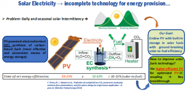
5) Solar power refineries. The aim is to combine PV and electrolysis to produce renewable-powered synthesised fuels, e.g. green hydrogen or syngas (mixture of CO and H2), contributing for the EU's energetic independence and its goal of achieving net-zero carbon-emission by 2050).

This TL deals with the development of cutting-edge functional and sustainable nanomaterials, nanostructures, and interfaces, the key one challenge on device performances, aiming to integrate cross-disciplinary solutions in inter-related areas based on the material's functionalities and physical properties, including 1D and 2D structures.
The primary aim is to develop smart materials and proper tailored interfaces for a wide range of applications:
1) Processing and Development of Materials for Energy, Optoelectronic, Electronic and Biomedical applications - ceramics for electronics, energy harvesting and storage and piezoelectric materials; multilayered MO films for magnetic sensors and MRAM; OLEDs and WOLEDs; wide and ultrawide bandgap semiconductors for solid-state light emitters; quantum technologies; memories; cutting-edge sensors; health applications; security and anti-counterfeiting; plasmonic interactions; nanoscale charge transport dynamics at devices interface.
2) Engineering of Smart Nanoparticles and 2D Materials: passivated and plasmonic solar cell architectures; (opto)electronic and magnetic properties of low-dimensional semiconductors (e.g. Si-NP) by doping, charge transport, defects, confinement, surface functionalization; luminescent nanomaterials for photocatalysis, bioimaging, plants in vivo monitoring and anti-counterfeiting; CVD graphene for bioapplications and GFETS for sensing; 2D materials and topological insulators; microwave synthesis of nanostructures for sensors, photocatalysis, and electrochromic devices.
3) Laser Processing and Surface modification: laser technology to produce and write at one step functional interfaces and surface engineering by promoting physical and chemical modifications on stacked layers (e.g. laser induced graphene (LIG) in eco-friendly substrates) for ITC (e.g. write sustainable PCB on biodegradable foils such as paper), bio, electrochemical and physical sensors; water splitting; energy production/storage and thermal management.
4) Neuromorphic and quantum technologies: memresistive and topological materials, single photon emitters, quantum bit holders and optical bioprobes, using ab-initio modelling and optical measurements; AI- and ML-assisted materials; topological behaviour of ultracold atoms.
5) Optical fibre nanoengineering: micromachining and functionalization of optical fibres using a NIR fs laser to produce sensors for multiparameter, based on Bragg gratings and FP interferometers; plasmonic sensors; modelling of topological insulators in photonic systems.
6) Natural and bioinspired nanomaterials: rheological behaviour of bacterial cultures; auto parts and bionic prosthetics; natural materials for ICT; functional inks for rigid and flexible substrates. Functional materials produced based on cellulose and chitin twisted structures: cellulose nanocrystals, water interactions and out-of-equilibrium structural colourful structures.

We are witnessing a major investment in preventive and precision medicine with excellent results in increasing longevity, while preserving the quality of life and public health. New and intelligent technologies are playing a fundamental role in the construction of these new medical tools, relieving the effort of health services and making them more specialised and effective. The two biggest contributions are the areas of diagnosis and therapy, isolated or combined (theranostics), with gains in prevention, disease detection and respective mitigation through efficient therapeutics. It is known that an early detection of the disease allows a better use of the applied therapies and in lesser ailments for patients. We are attentive to new approaches for diagnostics, vital signs monitoring and analyses, and therapeutics in clinical and preclinical fields. i3N research is aligned in this direction and with the public policies (national, EU and UN objectives), fostering the development, beyond the state of the art, of innovative biomedical solutions with high potential for disease prevention, precision medicine and for therapies, with new medical devices, medical imaging systems, functional biomaterials and regenerative medicine. The activity to be performed concerns:
1) Biomaterials, development of: functional materials, starting from nanoparticles and hybrids to nanocomposites to process scaffolds (hydrogels, aerogels, 3D printed structures) for tissue regeneration, bioactive and anti-microbial coatings, and nano-systems for cancer theranostics; and of hydroxyapatite and multifunctional bioactive glasses for bone regeneration; endo, exo, and endo-exo prostheses through additive methods, in ceramic and metallic materials, for the creation of prostheses that adapt more precisely to the individual needs of each patient.
2) Medical imaging, dosimetry and therapy, that includes: high resolution molecular imaging scanners: innovative preclinical PET and SPECT; BrainPET; and dedicated PET for accurate dosimetry in hadrontherapy; x-ray imaging (CT and EDXRFI), based on micropatterned gaseous detectors; hybrid medical dosimeters for interventional radiology; new theranostics combining encapsulated nanoparticles functionalized with positron emitter radionuclides and therapeutic agents.
3) Biosensors that includes: laser-induced graphene and its composites as electrochemical transducers for cost-effective, sustainable, miniaturised biosensors, namely for the detection of analytes with clinical interest (e.g. uric acid, dopamine, glucose, PSA, among others); vital signs monitoring systems, including machine learning approach and contactless, for clinical and health care, and home health care strategies; optical sensors based on several optical techniques: lab-on-fibre and lab-on-chip solutions for biosensing of different biomarkers in plasma, urine, saliva and sweat, namely, for heart failure, kidney diseases and stress biomarkers.
